SHARE
The Revolution of Solar Panels comes from Hybrid Technologies
The increasing concern for global warming effects is provoking that the researchers are looking for new ways of generating electricity. Today we bring you an improvement in the typical photovoltaic solar panels.
The two traditional ways of producing electricity from sunlight are photovoltaic and solar-thermal. Both have limitations and that is why there is an increasing need for hybrid technologies that take advantage of the benefits of each one. That is why a group of researchers at MIT has developed a device with higher efficiency than its predecessors.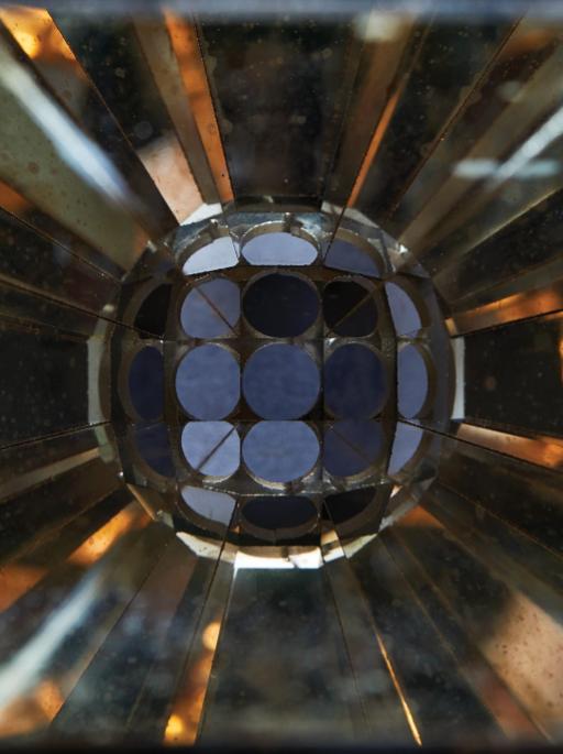
 The thermophotovoltaic efficiency depends on the spectral properties and temperature of the emitter. In order to produce enough absorbable energy, the emitter temperature should be high (around 1000ºC), so the researcher have varied the emitter-to-absorber area from 1 to 10 to achieve optimal performance. Increasing this ratio, they have managed to supply enough heat to reach this high temperature by increasing the level of irradiance.
The thermal resistance between the absorber and emitter is minimized by integrating the absorber and emitter on the same conductive silicon substrate such that heat is effectively delivered to the emitter via thermal spreading.
The thermophotovoltaic efficiency depends on the spectral properties and temperature of the emitter. In order to produce enough absorbable energy, the emitter temperature should be high (around 1000ºC), so the researcher have varied the emitter-to-absorber area from 1 to 10 to achieve optimal performance. Increasing this ratio, they have managed to supply enough heat to reach this high temperature by increasing the level of irradiance.
The thermal resistance between the absorber and emitter is minimized by integrating the absorber and emitter on the same conductive silicon substrate such that heat is effectively delivered to the emitter via thermal spreading.
 Finally, to reduce parasitic radioactive losses, they metalized the sides of the silicon substrate and inactive area around the nanotube absorber with tungsten, a relatively low-emissivity, high-temperature material, and incorporated a high-reflectivity silver-coated shield to recycle this parasitic radiation back to the device.
The benefits of this device are high efficiency, by harnessing the entire solar, scalability and compactness, because of their solid-state nature and dispatchability, owing to the ability to store energy using thermal or chemical means. With these improvements, they have managed to increase the total efficiency to 6.8% meanwhile previous devices only reached 1% but it is supposed to double the efficiency of conventional photovoltaics.
You can also help the environment by solving our last engineering challenge. Can you provide a solution?
Join our engineering community here
Finally, to reduce parasitic radioactive losses, they metalized the sides of the silicon substrate and inactive area around the nanotube absorber with tungsten, a relatively low-emissivity, high-temperature material, and incorporated a high-reflectivity silver-coated shield to recycle this parasitic radiation back to the device.
The benefits of this device are high efficiency, by harnessing the entire solar, scalability and compactness, because of their solid-state nature and dispatchability, owing to the ability to store energy using thermal or chemical means. With these improvements, they have managed to increase the total efficiency to 6.8% meanwhile previous devices only reached 1% but it is supposed to double the efficiency of conventional photovoltaics.
You can also help the environment by solving our last engineering challenge. Can you provide a solution?
Join our engineering community here

How it works
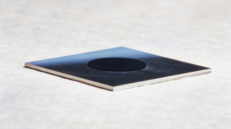
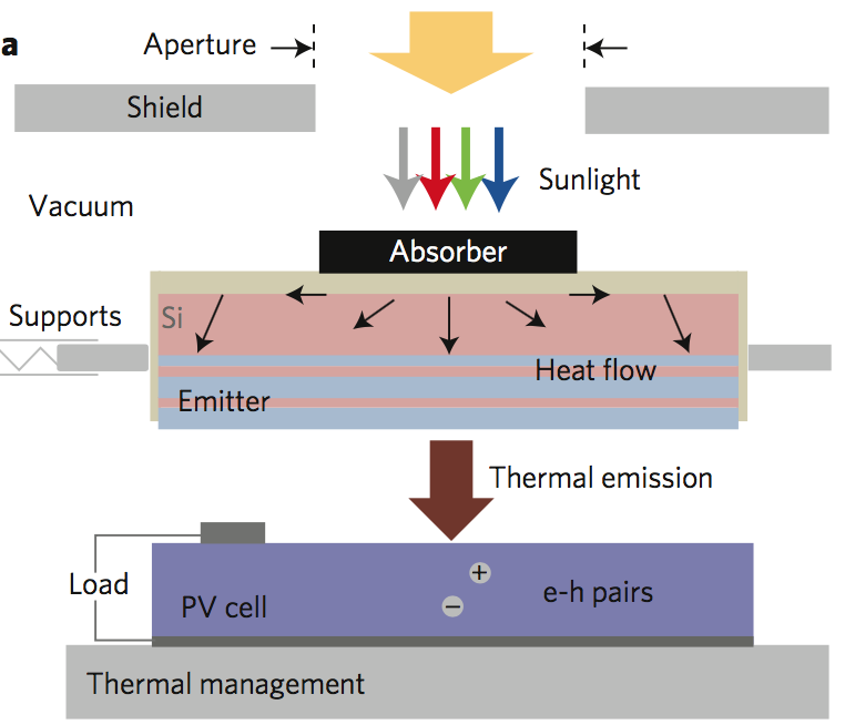
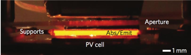
First, it converts sunlight into thermal energy. Then, this thermal energy is turned to energies above the photovoltaic bandgap in order to exploit the maximum portion of the solar spectrum efficiently. This process is done with a hot absorber-emitter. On the one hand, the absorber is formed by a multiwalled carbon nanotube array with high-temperature stability in a vacuum and nearly ideal absorptance, crucial for absorbing highly concentrated irradiance at elevated emitter-to-absorber area ratios. On the other hand, the emitter is composed of a multilayer Si/SiO2 structure, specifically of five alternating layers of silicon and SiO2, that improves the spectral matching between the emittance of the emitter and the internal quantum efficiency of the photovoltaic. These materials were chosen for ease of fabrication and high-temperature compatibility with the silicon substrate. The thermophotovoltaic efficiency depends on the spectral properties and temperature of the emitter. In order to produce enough absorbable energy, the emitter temperature should be high (around 1000ºC), so the researcher have varied the emitter-to-absorber area from 1 to 10 to achieve optimal performance. Increasing this ratio, they have managed to supply enough heat to reach this high temperature by increasing the level of irradiance.
The thermal resistance between the absorber and emitter is minimized by integrating the absorber and emitter on the same conductive silicon substrate such that heat is effectively delivered to the emitter via thermal spreading.
The thermophotovoltaic efficiency depends on the spectral properties and temperature of the emitter. In order to produce enough absorbable energy, the emitter temperature should be high (around 1000ºC), so the researcher have varied the emitter-to-absorber area from 1 to 10 to achieve optimal performance. Increasing this ratio, they have managed to supply enough heat to reach this high temperature by increasing the level of irradiance.
The thermal resistance between the absorber and emitter is minimized by integrating the absorber and emitter on the same conductive silicon substrate such that heat is effectively delivered to the emitter via thermal spreading.
 Finally, to reduce parasitic radioactive losses, they metalized the sides of the silicon substrate and inactive area around the nanotube absorber with tungsten, a relatively low-emissivity, high-temperature material, and incorporated a high-reflectivity silver-coated shield to recycle this parasitic radiation back to the device.
The benefits of this device are high efficiency, by harnessing the entire solar, scalability and compactness, because of their solid-state nature and dispatchability, owing to the ability to store energy using thermal or chemical means. With these improvements, they have managed to increase the total efficiency to 6.8% meanwhile previous devices only reached 1% but it is supposed to double the efficiency of conventional photovoltaics.
You can also help the environment by solving our last engineering challenge. Can you provide a solution?
Join our engineering community here
Finally, to reduce parasitic radioactive losses, they metalized the sides of the silicon substrate and inactive area around the nanotube absorber with tungsten, a relatively low-emissivity, high-temperature material, and incorporated a high-reflectivity silver-coated shield to recycle this parasitic radiation back to the device.
The benefits of this device are high efficiency, by harnessing the entire solar, scalability and compactness, because of their solid-state nature and dispatchability, owing to the ability to store energy using thermal or chemical means. With these improvements, they have managed to increase the total efficiency to 6.8% meanwhile previous devices only reached 1% but it is supposed to double the efficiency of conventional photovoltaics.
You can also help the environment by solving our last engineering challenge. Can you provide a solution?
Join our engineering community here